W25Q64 SPI flash board
See the latest version. This site is no longer maintained.
See the latest version for up-to-date documentation. Docs have been completely reworked and moved to a new location. The new site is more user-friendly and searchable. It's also easier for the developers to work with.
A cheap W25Q64 SPI flash board that adds 8 megabytes of storage to your project:
- Cost: ~$2
- Size: 8MB
- VCC: 2.7 - 3.6V
- It includes pull-ups on the /HOLD & /WP (write protect) pins
- 32768 programmable pages of 256-bytes each. Up to 256 bytes can be programmed at a time.
- Pages can be erased in groups of 16 (4KB sector erase), groups of 128 (32KB block erase), groups of 256 (64KB block erase) or the entire chip (chip erase).
- Considering it might be a Chinese clone purchased from AliExpress or a similar site, here's the maximum speed I recommend: ~10MHz (Standard SPI)
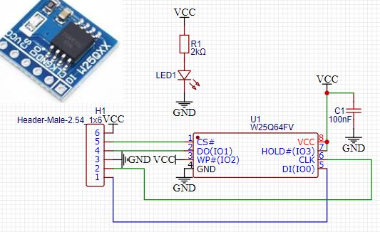
Connections
| Bus Pirate | W25Q64 board | Description |
|---|---|---|
| CS | CS | Chip select |
| CDI | DO | MISO Controller Data In |
| CDO | DI | MOSI Controller Data Out |
| SCLK | CLK | SPI Clock |
| Vout/Vref | VCC | 3.3volt power supply |
| GND | GND | Ground |
Setup
While the chip has an impressive top speed of 104MHz, it's probably unreliable at high speeds because of the length of the Bus Pirate cable and possibly low quality clone board from AliExpress. We're going to be very conservative and operate at:
- 3V3, 100kHz.
- Max current: 50ma.
If you're using the chip alone (socket adapter, breadboard...) you must connect /HOLD & /WP to VCC (3.3volts).
Mode selection
1. HiZ
2. 1-WIRE
3. UART
4. I2C
5. SPI
6. LED
x. Exit
Mode > 5
SPI speed
1 to 62500KHz
x. Exit
KHz (100KHz*) >
Data bits
4 to 8 bits
x. Exit
Bits (8*) >
Clock polarity
1. Idle LOW*
2. Idle HIGH
x. Exit
Polarity (1) >
Clock phase
1. LEADING edge*
2. TRAILING edge
x. Exit
Phase (1) >
Chip select
1. Active HIGH (CS)
2. Active LOW (/CS)*
x. Exit
CS (2) >
Actual speed: 122KHz
Mode: SPI
SPI> W
Power supply
Volts (0.80V-5.00V)
x to exit (3.30) >
3.30V requested, closest value: 3.30V
Set current limit?
y
Maximum current (0mA-500mA)
x to exit (100.00) > 50
50.0mA requested, closest value: 50.0mA
Power supply:Enabled
Vreg output: 3.3V, Vref/Vout pin: 3.3V, Current sense: 5.8mA
SPI>
- Use the
mmode command and select SPI - Configure SPI for 100kHz and 8bits of data
- Enable the onboard power supply with the
Wcommand, and configure it for 3.3volts output. - Select a current limit of at least 50mA.
Write 256 bytes
We will write 256 ASCII characters 'i' (0x69) at the memory address 0x00. Following this, we will read the content to verify that the bytes have been correctly written.
Enable writes
CS Enabled
TX: 0x06
CS Disabled
SPI>
The 'Write Enable' command 0x06 must be sent before write and erase commands will be accepted. This prevents accidental erasures or overwrites of your valuable data. This command must be sent before any write, erase or configuration command.
[- Start of SPI transaction. Lowers the CS pin to ground.0x06- Write Enable instruction.]- End of SPI transaction. Raises the CS pin to 3.3volts.
Verify write enable
CS Enabled
TX: 0x05
RX: 0x02
CS Disabled
SPI>
| S7 | S6 | S5 | S4 | S3 | S2 | S1 | S0 |
|---|---|---|---|---|---|---|---|
| SRP0 | SEC | TB | BP2 | BP1 | BP0 | WEL | BUSY |
Read Status Register 0x05 is used to verify the 'Write Enable' instruction 0x06 was correctly received.
[- Start of SPI transaction. Lowers the CS pin to ground.0x05- Read Status Register instruction.r:1- Read 1 byte.]- End of SPI transaction. Raises the CS pin to 3.3volts.
Response 0x02 indicates that the write enable bit (S1) is set to 1 (0x02=0b00000010).
Erase sector
CS Enabled
TX: 0x06
CS Disabled
SPI> [0x20 0x00 0x00 0x00]
CS Enabled
TX: 0x20 0x00 0x00 0x00
CS Disabled
SPI>
Flash works by flipping 1s in the memory to 0. Writing a location twice will simply flip more bits from 1 to 0, but will not flip 0 to 1. The erase sector command 0x20 is used to flip all bits in a 4000 byte sector from 0 to 1, after which we can write new data.
The erase sector command is followed by a three byte address of the location to begin erasing 4000 bytes. It's not possible to begin erasing just anywhere. The 4000 byte sectors are 'aligned' in bocks. The first sector begins at 0, the next at 4000, the next at 8000 and so on. We'll erase the first sector from 0 to 3999.
A write enable command must be sent before the erase sector command will be accepted.
[- Start of SPI transaction. Lowers the CS pin to ground.0x06- Write Enable instruction.]- End of SPI transaction. Raises the CS pin to 3.3volts.[- Start of SPI transaction. Lowers the CS pin to ground.0x20- Erase Sector instruction.0x00 0x00 0x00- Address 0x00.]- End of SPI transaction. Raises the CS pin to 3.3volts.
Flash needs to be erased before it can be rewritten. Flash is erased in sectors, blocks or the entire chip.
Verify erase sector
CS Enabled
TX: 0x03 0x00 0x00 0x00
RX: 0xFF 0xFF 0xFF 0xFF 0xFF 0xFF 0xFF 0xFF
0xFF 0xFF 0xFF 0xFF 0xFF 0xFF 0xFF 0xFF
0xFF 0xFF 0xFF 0xFF 0xFF 0xFF 0xFF 0xFF
0xFF 0xFF 0xFF 0xFF 0xFF 0xFF 0xFF 0xFF
0xFF 0xFF 0xFF 0xFF 0xFF 0xFF 0xFF 0xFF
0xFF 0xFF 0xFF 0xFF 0xFF 0xFF 0xFF 0xFF
0xFF 0xFF 0xFF 0xFF 0xFF 0xFF 0xFF 0xFF
0xFF 0xFF 0xFF 0xFF 0xFF 0xFF 0xFF 0xFF
0xFF 0xFF 0xFF 0xFF 0xFF 0xFF 0xFF 0xFF
0xFF 0xFF 0xFF 0xFF 0xFF 0xFF 0xFF 0xFF
0xFF 0xFF 0xFF 0xFF 0xFF 0xFF 0xFF 0xFF
0xFF 0xFF 0xFF 0xFF 0xFF 0xFF 0xFF 0xFF
0xFF 0xFF 0xFF 0xFF 0xFF 0xFF 0xFF 0xFF
0xFF 0xFF 0xFF 0xFF 0xFF 0xFF 0xFF 0xFF
0xFF 0xFF 0xFF 0xFF 0xFF 0xFF 0xFF 0xFF
0xFF 0xFF 0xFF 0xFF 0xFF 0xFF 0xFF 0xFF
0xFF 0xFF 0xFF 0xFF 0xFF 0xFF 0xFF 0xFF
0xFF 0xFF 0xFF 0xFF 0xFF 0xFF 0xFF 0xFF
0xFF 0xFF 0xFF 0xFF 0xFF 0xFF 0xFF 0xFF
0xFF 0xFF 0xFF 0xFF 0xFF 0xFF 0xFF 0xFF
0xFF 0xFF 0xFF 0xFF 0xFF 0xFF 0xFF 0xFF
0xFF 0xFF 0xFF 0xFF 0xFF 0xFF 0xFF 0xFF
0xFF 0xFF 0xFF 0xFF 0xFF 0xFF 0xFF 0xFF
0xFF 0xFF 0xFF 0xFF 0xFF 0xFF 0xFF 0xFF
0xFF 0xFF 0xFF 0xFF 0xFF 0xFF 0xFF 0xFF
0xFF 0xFF 0xFF 0xFF 0xFF 0xFF 0xFF 0xFF
0xFF 0xFF 0xFF 0xFF 0xFF 0xFF 0xFF 0xFF
0xFF 0xFF 0xFF 0xFF 0xFF 0xFF 0xFF 0xFF
0xFF 0xFF 0xFF 0xFF 0xFF 0xFF 0xFF 0xFF
0xFF 0xFF 0xFF 0xFF 0xFF 0xFF 0xFF 0xFF
0xFF 0xFF 0xFF 0xFF 0xFF 0xFF 0xFF 0xFF
0xFF 0xFF 0xFF 0xFF 0xFF 0xFF 0xFF 0xFF
CS Disabled
SPI>
We'll use the read data command 0x03 to verify that the sector has been erased to all 1s (0xff). The command is followed by a three byte address of the location to begin reading 256 bytes. We'll read the first 256 bytes from address 0x00.
[- Start of SPI transaction. Lowers the CS pin to ground.0x03- Read Data instruction.0x00 0x00 0x00- Address 0x00.r:256- Read 256 bytes.]- End of SPI transaction. Raises the CS pin to 3.3volts.
Enable writes and verify
CS Enabled
TX: 0x06
CS Disabled
SPI> [0x05 r:1]
CS Enabled
TX: 0x05
RX: 0x02
SPI>
CS Disabled
Use the write enable command 0x06 to enable writes. Verify the write enable bit is set to 1 (0x02=0b00000010) using the read status register command 0x05.
Write data
CS Enabled
TX: 0x02 0x00 0x00 0x00 0x69 0x69 0x69 0x69
0x69 0x69 0x69 0x69 0x69 0x69 0x69 0x69
0x69 0x69 0x69 0x69 0x69 0x69 0x69 0x69
0x69 0x69 0x69 0x69 0x69 0x69 0x69 0x69
0x69 0x69 0x69 0x69 0x69 0x69 0x69 0x69
0x69 0x69 0x69 0x69 0x69 0x69 0x69 0x69
0x69 0x69 0x69 0x69 0x69 0x69 0x69 0x69
0x69 0x69 0x69 0x69 0x69 0x69 0x69 0x69
0x69 0x69 0x69 0x69 0x69 0x69 0x69 0x69
0x69 0x69 0x69 0x69 0x69 0x69 0x69 0x69
0x69 0x69 0x69 0x69 0x69 0x69 0x69 0x69
0x69 0x69 0x69 0x69 0x69 0x69 0x69 0x69
0x69 0x69 0x69 0x69 0x69 0x69 0x69 0x69
0x69 0x69 0x69 0x69 0x69 0x69 0x69 0x69
0x69 0x69 0x69 0x69 0x69 0x69 0x69 0x69
0x69 0x69 0x69 0x69 0x69 0x69 0x69 0x69
0x69 0x69 0x69 0x69 0x69 0x69 0x69 0x69
0x69 0x69 0x69 0x69 0x69 0x69 0x69 0x69
0x69 0x69 0x69 0x69 0x69 0x69 0x69 0x69
0x69 0x69 0x69 0x69 0x69 0x69 0x69 0x69
0x69 0x69 0x69 0x69 0x69 0x69 0x69 0x69
0x69 0x69 0x69 0x69 0x69 0x69 0x69 0x69
0x69 0x69 0x69 0x69 0x69 0x69 0x69 0x69
0x69 0x69 0x69 0x69 0x69 0x69 0x69 0x69
0x69 0x69 0x69 0x69 0x69 0x69 0x69 0x69
0x69 0x69 0x69 0x69 0x69 0x69 0x69 0x69
0x69 0x69 0x69 0x69 0x69 0x69 0x69 0x69
0x69 0x69 0x69 0x69 0x69 0x69 0x69 0x69
0x69 0x69 0x69 0x69 0x69 0x69 0x69 0x69
0x69 0x69 0x69 0x69 0x69 0x69 0x69 0x69
0x69 0x69 0x69 0x69 0x69 0x69 0x69 0x69
0x69 0x69 0x69 0x69 0x69 0x69 0x69 0x69
0x69 0x69 0x69 0x69
CS Disabled
SPI>
Use the page program command 0x02 to write 256 bytes of data to address 0x00. The command is followed by a three byte address of the location to begin writing 256 bytes 0x00 0x00 0x00. The data to be written i (0x69) follows the address.
[- Start of SPI transaction. Lowers the CS pin to ground.0x02- Page Program instruction.0x00 0x00 0x00- Address to begin writing: 0x00.0x69:256- Write 256 bytes of data. The data to be written isi(0x69).]- End of SPI transaction. Raises the CS pin to 3.3volts.
The write enable command 0x06 must be send before writing data to the chip. Write up to 256 bytes at a time. If more than 256 bytes are sent, the internal buffer will circle back to the beginning of the page and overwrite previously sent data.
Read data
CS Enabled
TX: 0x03 0x00 0x00 0x00
RX: 0x69 0x69 0x69 0x69 0x69 0x69 0x69 0x69
0x69 0x69 0x69 0x69 0x69 0x69 0x69 0x69
0x69 0x69 0x69 0x69 0x69 0x69 0x69 0x69
0x69 0x69 0x69 0x69 0x69 0x69 0x69 0x69
0x69 0x69 0x69 0x69 0x69 0x69 0x69 0x69
0x69 0x69 0x69 0x69 0x69 0x69 0x69 0x69
0x69 0x69 0x69 0x69 0x69 0x69 0x69 0x69
0x69 0x69 0x69 0x69 0x69 0x69 0x69 0x69
0x69 0x69 0x69 0x69 0x69 0x69 0x69 0x69
0x69 0x69 0x69 0x69 0x69 0x69 0x69 0x69
0x69 0x69 0x69 0x69 0x69 0x69 0x69 0x69
0x69 0x69 0x69 0x69 0x69 0x69 0x69 0x69
0x69 0x69 0x69 0x69 0x69 0x69 0x69 0x69
0x69 0x69 0x69 0x69 0x69 0x69 0x69 0x69
0x69 0x69 0x69 0x69 0x69 0x69 0x69 0x69
0x69 0x69 0x69 0x69 0x69 0x69 0x69 0x69
0x69 0x69 0x69 0x69 0x69 0x69 0x69 0x69
0x69 0x69 0x69 0x69 0x69 0x69 0x69 0x69
0x69 0x69 0x69 0x69 0x69 0x69 0x69 0x69
0x69 0x69 0x69 0x69 0x69 0x69 0x69 0x69
0x69 0x69 0x69 0x69 0x69 0x69 0x69 0x69
0x69 0x69 0x69 0x69 0x69 0x69 0x69 0x69
0x69 0x69 0x69 0x69 0x69 0x69 0x69 0x69
0x69 0x69 0x69 0x69 0x69 0x69 0x69 0x69
0x69 0x69 0x69 0x69 0x69 0x69 0x69 0x69
0x69 0x69 0x69 0x69 0x69 0x69 0x69 0x69
0x69 0x69 0x69 0x69 0x69 0x69 0x69 0x69
0x69 0x69 0x69 0x69 0x69 0x69 0x69 0x69
0x69 0x69 0x69 0x69 0x69 0x69 0x69 0x69
0x69 0x69 0x69 0x69 0x69 0x69 0x69 0x69
0x69 0x69 0x69 0x69 0x69 0x69 0x69 0x69
0x69 0x69 0x69 0x69 0x69 0x69 0x69 0x69
CS Disabled
SPI>
To confirm the data was written, we use the 'Read Data' instruction 0x03 once again.
[- Start of SPI transaction. Lowers the CS pin to ground.0x03- Read Data instruction.0x00 0x00 0x00- Address to begin reading: 0x00.r:256- Read 256 bytes of data.]- End of SPI transaction. Raises the CS pin to 3.3volts.
If the writing/reading process fails, check all connections. /HOLD & /WP pins must be connected to 3.3 volts.
Get Bus Pirate 5
- Browse Complete Bus Pirate hardware collection
- Bus Pirate 5 REV10 with enclosure
- Probe Cable Kit
- Auxiliary Cable Kit
- Quick Connect Adapter