SPI flash chips
See the latest version. This site is no longer maintained.
See the latest version for up-to-date documentation. Docs have been completely reworked and moved to a new location. The new site is more user-friendly and searchable. It's also easier for the developers to work with.
Eight pin SPI flash chips are a cheap and easy way to add storage to your project. They're available in sizes from 1MB to 128MB, and can be used to store data, firmware, or even a filesystem. They're commonly found on PC motherboards for storing BIOS, FPGAs for storing bitstreams, and even the Bus Pirate for storing the firmware.
Connections
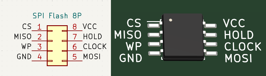
| Bus Pirate | SPI Flash | Description |
|---|---|---|
| CS/IO5 | CS | Chip select |
| MISO/IO4 | DO | MISO Controller Data In |
| MOSI/IO7 | DI | MOSI Controller Data Out |
| CLK/IO6 | CLK | SPI Clock |
| WP/IO3 | WP | Write Protect, HIGH to disable |
| HOLD/IO2 | HOLD | Hold, HIGH to disable |
| Vout | VCC | 3.3volt power supply |
| GND | GND | Ground |
Connect the Bus Pirate to the SPI flash chip as shown in the table above. Don't forget the the write protect (WP) and hold pins, or the chip may not behave normally.
SPI Flash Adapters
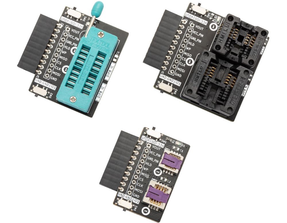
SPI flash adapters for SOP8, WSON8, and DIP8 chips are available for Bus Pirate 5. Connect SPI flash chips to the Bus Pirate quickly and easily.
Setup
While some flash chips have an impressive top speed of 104MHz, it's unreliable at high speeds because of the length of the Bus Pirate cable and other factors. We're going to be very conservative and operate at:
- 3V3, 100kHz.
- Max current: 50ma.
Mode selection
1. HiZ
2. 1-WIRE
3. UART
4. I2C
5. SPI
6. LED
x. Exit
Mode > 5
SPI speed
1 to 62500KHz
x. Exit
KHz (100KHz*) >
Data bits
4 to 8 bits
x. Exit
Bits (8*) >
Clock polarity
1. Idle LOW*
2. Idle HIGH
x. Exit
Polarity (1) >
Clock phase
1. LEADING edge*
2. TRAILING edge
x. Exit
Phase (1) >
Chip select
1. Active HIGH (CS)
2. Active LOW (/CS)*
x. Exit
CS (2) >
Actual speed: 122KHz
Mode: SPI
SPI> W
Power supply
Volts (0.80V-5.00V)
x to exit (3.30) >
3.30V requested, closest value: 3.30V
Set current limit?
y
Maximum current (0mA-500mA)
x to exit (100.00) > 50
50.0mA requested, closest value: 50.0mA
Power supply:Enabled
Vreg output: 3.3V, Vref/Vout pin: 3.3V, Current sense: 5.8mA
SPI>
- Use the
mmode command and select SPI - Configure SPI for 100kHz and 8bits of data, hit enter to accept the defaults
- Enable the onboard power supply with the
Wcommand, and configure it for 3.3volts output. - Select a current limit of at least 50mA.
WP and HOLD pins
Pull-up resistors: Enabled (10K ohms @ 3.3V)
SPI>
Most SPI flash chips have a write protect pin (WP) that prevents accidental writes, and a hold pin (HOLD) that pauses the chip. The HOLD pin must be held high or the chip won't respond. WP must be held high or the chip will be read only. Often the chip will not respond if is WP is left floating, so be sure to hold it high (write enabled) or low (write disabled).
Two ways to correctly hold the WP and HOLD pins high for normal chip operation:
P- Enable pull-up resistors to hold the pins highA 2; A 3- Use Auxiliary pin control to set IO2 and IO3 high
Ensure WP and HOLD pins are held high or the chip may not respond.
Identify the chip
SPI flash chip commands are loosely standardized on some historical trends, but each manufacturer tends to add their own extensions.
We'll try to use the most common commands, but not all chips will respond to all commands!
Reset ID
CS Enabled
TX: 0xB9
Delay: 10ms
TX: 0xAB 0x00 0x00 0x00
RX: 0xEF
CS Disabled
SPI>
The 'Reset ID' command 0xAB is used to read the device ID of the flash chip immediately after reset. The command is followed by a single byte response.
[0xb9]- Reset the SPI flash chipD:10- Delay 10ms[0xab 0x00:3 r]- Send the 'Reset ID' command0xABfollowed by three byte dummy bytes0x00:3.rto read a one byte response.
The response 0x13 is the device ID of the flash chip. There's no standard, and about the only way to find it is through datasheets. This is primarily a way for a device to determine which flash chip is present among several known variants.
Read Electronic Manufacturer ID
CS Enabled
TX: 0x90 0x00 0x00 0x00
RX: 0x13 0xEF
CS Disabled
SPI>
The 'Read Electronic Manufacturer ID' command 0x90 is used to read the device ID and manufacturer ID of the flash chip. The command is followed by a two byte response.
[0x90 0x00:3 r:2]- Send the 'Read Electronic Manufacturer ID' command0x90followed by three byte dummy bytes0x00:3.r:2to read a two byte response.
The response 0x13 is the device ID of the flash chip, same as the Reset ID command.
0xEF is the manufacturer ID: Winbond. The manufacturer ID is a unique value assigned to each manufacturer - except they ran out of IDs and started duplicating ages ago so it's not super useful. JEDEC maintains a list of IDs (free but agreement required) that can help narrow it down somewhat.
Read JEDEC ID
CS Enabled
TX: 0x9F
RX: 0xEF 0x40 0x14
CS Disabled
SPI>
The 'Read JEDEC ID' command 0x9F is used to read the manufacturer ID, memory type ID, and capacity ID of the flash chip. The command is followed by a three byte response.
[0x9F r:3]- Send the 'Read JEDEC ID' command0x9F.r:3to read a three byte response.
The manufacturer ID is 0xEF, the memory type ID is 0x40, and the capacity ID is 0x14. Manufactures use different systems to encode memory type and capacity ID for each chip. There is no universal standard for these values, and they can vary between manufacturers and even between different chips from the same manufacturer.
Read SFDP tables
CS Enabled
TX: 0x5A 0x00 0x00 0x00
RX: 0x50 0x44 0x46 0x53 0x05 0x01 0x00 0xFF
We've tried three ID commands that don't give us a ton of useful information. The Serial Flash Discoverable Parameters (SFDP) tables are a newer standard that provides a lot more information about the flash chip.
[0x5A 0x00:4 r:8]- Send the 'Read SFDP' command0x5Afollowed by four address bytes0x00:4.r:8to read 8 bytes from address 0x00.
The read SFDP table command includes a 4 byte address where the chip will start reading inside the tables. If SFDP tables are present, the first 4 bytes will contain the signature 'SFDP'.
| Byte | Value | Description |
|---|---|---|
| 0 | 0x50 | 'P' |
| 1 | 0x44 | 'D' |
| 2 | 0x46 | 'F' |
| 3 | 0x53 | 'S' |
| 4 | 0x05 | Minor revision number |
| 5 | 0x01 | Major revision number |
| 6 | 0x00 | Number of parameter headers (+1) |
| 7 | 0xFF | End of parameter headers |
The first four bytes here are the SFDP signature: 0x50 0x44 0x46 0x53. This is the ASCII representation of 'PDFS'. Values are stored in big-endian format, so reverse that to get SFDP.
Use the Bus Pirate = command to convert numerical values to ASCII: = 0x50
The next byte is the minor revision number (0x05), followed by the major revision number (0x01). This is a JEDEC v1.5 SFDP table. The number of parameter headers byte (0x00) plus 1 = 1 available Headers. The table ends with 0xFF.
If we continue retrieving SFDP tables we can find useful information like the chip capacity, acceptable voltage range, and even commands for controlling the chip. Retrieving and decoding the full SFDP table is beyond the scope of this intro guide, but you can see the full process step by step when we developed the flash read/write/erase command.
Write 256 bytes
We will write 256 ASCII characters 'i' (0x69) at the memory address 0x00. Following this, we will read the content to verify that the bytes have been correctly written.
Enable writes
CS Enabled
TX: 0x06
CS Disabled
SPI>
The 'Write Enable' command 0x06 must be sent before write and erase commands will be accepted. This prevents accidental erasures or overwrites of your valuable data. This command must be sent before any write, erase or configuration command.
[- Start of SPI transaction. Lowers the CS pin to ground.0x06- Write Enable instruction.]- End of SPI transaction. Raises the CS pin to 3.3volts.
Verify write enable
CS Enabled
TX: 0x05
RX: 0x02
CS Disabled
SPI>
| S7 | S6 | S5 | S4 | S3 | S2 | S1 | S0 |
|---|---|---|---|---|---|---|---|
| SRP0 | SEC | TB | BP2 | BP1 | BP0 | WEL | BUSY |
Read Status Register 0x05 is used to verify the 'Write Enable' instruction 0x06 was correctly received.
[- Start of SPI transaction. Lowers the CS pin to ground.0x05- Read Status Register instruction.r:1- Read 1 byte.]- End of SPI transaction. Raises the CS pin to 3.3volts.
Response 0x02 indicates that the write enable bit (S1) is set to 1 (0x02=0b00000010).
Erase sector
CS Enabled
TX: 0x06
CS Disabled
SPI> [0x20 0x00 0x00 0x00]
CS Enabled
TX: 0x20 0x00 0x00 0x00
CS Disabled
SPI>
Flash works by flipping 1s in the memory to 0. Writing a location twice will simply flip more bits from 1 to 0, but will not flip 0 to 1. The erase sector command 0x20 is used to flip all bits in a 4000 byte sector from 0 to 1, after which we can write new data.
The erase sector command is followed by a three byte address of the location to begin erasing 4000 bytes. It's not possible to begin erasing just anywhere. The 4000 byte sectors are 'aligned' in bocks. The first sector begins at 0, the next at 4000, the next at 8000 and so on. We'll erase the first sector from 0 to 3999.
A write enable command must be sent before the erase sector command will be accepted.
[- Start of SPI transaction. Lowers the CS pin to ground.0x06- Write Enable instruction.]- End of SPI transaction. Raises the CS pin to 3.3volts.[- Start of SPI transaction. Lowers the CS pin to ground.0x20- Erase Sector instruction.0x00 0x00 0x00- Address 0x00.]- End of SPI transaction. Raises the CS pin to 3.3volts.
Flash needs to be erased before it can be rewritten. Flash is erased in sectors, blocks or the entire chip.
Verify erase sector
CS Enabled
TX: 0x03 0x00 0x00 0x00
RX: 0xFF 0xFF 0xFF 0xFF 0xFF 0xFF 0xFF 0xFF
0xFF 0xFF 0xFF 0xFF 0xFF 0xFF 0xFF 0xFF
0xFF 0xFF 0xFF 0xFF 0xFF 0xFF 0xFF 0xFF
0xFF 0xFF 0xFF 0xFF 0xFF 0xFF 0xFF 0xFF
0xFF 0xFF 0xFF 0xFF 0xFF 0xFF 0xFF 0xFF
0xFF 0xFF 0xFF 0xFF 0xFF 0xFF 0xFF 0xFF
0xFF 0xFF 0xFF 0xFF 0xFF 0xFF 0xFF 0xFF
0xFF 0xFF 0xFF 0xFF 0xFF 0xFF 0xFF 0xFF
0xFF 0xFF 0xFF 0xFF 0xFF 0xFF 0xFF 0xFF
0xFF 0xFF 0xFF 0xFF 0xFF 0xFF 0xFF 0xFF
0xFF 0xFF 0xFF 0xFF 0xFF 0xFF 0xFF 0xFF
0xFF 0xFF 0xFF 0xFF 0xFF 0xFF 0xFF 0xFF
0xFF 0xFF 0xFF 0xFF 0xFF 0xFF 0xFF 0xFF
0xFF 0xFF 0xFF 0xFF 0xFF 0xFF 0xFF 0xFF
0xFF 0xFF 0xFF 0xFF 0xFF 0xFF 0xFF 0xFF
0xFF 0xFF 0xFF 0xFF 0xFF 0xFF 0xFF 0xFF
0xFF 0xFF 0xFF 0xFF 0xFF 0xFF 0xFF 0xFF
0xFF 0xFF 0xFF 0xFF 0xFF 0xFF 0xFF 0xFF
0xFF 0xFF 0xFF 0xFF 0xFF 0xFF 0xFF 0xFF
0xFF 0xFF 0xFF 0xFF 0xFF 0xFF 0xFF 0xFF
0xFF 0xFF 0xFF 0xFF 0xFF 0xFF 0xFF 0xFF
0xFF 0xFF 0xFF 0xFF 0xFF 0xFF 0xFF 0xFF
0xFF 0xFF 0xFF 0xFF 0xFF 0xFF 0xFF 0xFF
0xFF 0xFF 0xFF 0xFF 0xFF 0xFF 0xFF 0xFF
0xFF 0xFF 0xFF 0xFF 0xFF 0xFF 0xFF 0xFF
0xFF 0xFF 0xFF 0xFF 0xFF 0xFF 0xFF 0xFF
0xFF 0xFF 0xFF 0xFF 0xFF 0xFF 0xFF 0xFF
0xFF 0xFF 0xFF 0xFF 0xFF 0xFF 0xFF 0xFF
0xFF 0xFF 0xFF 0xFF 0xFF 0xFF 0xFF 0xFF
0xFF 0xFF 0xFF 0xFF 0xFF 0xFF 0xFF 0xFF
0xFF 0xFF 0xFF 0xFF 0xFF 0xFF 0xFF 0xFF
0xFF 0xFF 0xFF 0xFF 0xFF 0xFF 0xFF 0xFF
CS Disabled
SPI>
We'll use the read data command 0x03 to verify that the sector has been erased to all 1s (0xff). The command is followed by a three byte address of the location to begin reading 256 bytes. We'll read the first 256 bytes from address 0x00.
[- Start of SPI transaction. Lowers the CS pin to ground.0x03- Read Data instruction.0x00 0x00 0x00- Address 0x00.r:256- Read 256 bytes.]- End of SPI transaction. Raises the CS pin to 3.3volts.
Enable writes and verify
CS Enabled
TX: 0x06
CS Disabled
SPI> [0x05 r:1]
CS Enabled
TX: 0x05
RX: 0x02
SPI>
CS Disabled
Use the write enable command 0x06 to enable writes. Verify the write enable bit is set to 1 (0x02=0b00000010) using the read status register command 0x05.
Write data
CS Enabled
TX: 0x02 0x00 0x00 0x00 0x69 0x69 0x69 0x69
0x69 0x69 0x69 0x69 0x69 0x69 0x69 0x69
0x69 0x69 0x69 0x69 0x69 0x69 0x69 0x69
0x69 0x69 0x69 0x69 0x69 0x69 0x69 0x69
0x69 0x69 0x69 0x69 0x69 0x69 0x69 0x69
0x69 0x69 0x69 0x69 0x69 0x69 0x69 0x69
0x69 0x69 0x69 0x69 0x69 0x69 0x69 0x69
0x69 0x69 0x69 0x69 0x69 0x69 0x69 0x69
0x69 0x69 0x69 0x69 0x69 0x69 0x69 0x69
0x69 0x69 0x69 0x69 0x69 0x69 0x69 0x69
0x69 0x69 0x69 0x69 0x69 0x69 0x69 0x69
0x69 0x69 0x69 0x69 0x69 0x69 0x69 0x69
0x69 0x69 0x69 0x69 0x69 0x69 0x69 0x69
0x69 0x69 0x69 0x69 0x69 0x69 0x69 0x69
0x69 0x69 0x69 0x69 0x69 0x69 0x69 0x69
0x69 0x69 0x69 0x69 0x69 0x69 0x69 0x69
0x69 0x69 0x69 0x69 0x69 0x69 0x69 0x69
0x69 0x69 0x69 0x69 0x69 0x69 0x69 0x69
0x69 0x69 0x69 0x69 0x69 0x69 0x69 0x69
0x69 0x69 0x69 0x69 0x69 0x69 0x69 0x69
0x69 0x69 0x69 0x69 0x69 0x69 0x69 0x69
0x69 0x69 0x69 0x69 0x69 0x69 0x69 0x69
0x69 0x69 0x69 0x69 0x69 0x69 0x69 0x69
0x69 0x69 0x69 0x69 0x69 0x69 0x69 0x69
0x69 0x69 0x69 0x69 0x69 0x69 0x69 0x69
0x69 0x69 0x69 0x69 0x69 0x69 0x69 0x69
0x69 0x69 0x69 0x69 0x69 0x69 0x69 0x69
0x69 0x69 0x69 0x69 0x69 0x69 0x69 0x69
0x69 0x69 0x69 0x69 0x69 0x69 0x69 0x69
0x69 0x69 0x69 0x69 0x69 0x69 0x69 0x69
0x69 0x69 0x69 0x69 0x69 0x69 0x69 0x69
0x69 0x69 0x69 0x69 0x69 0x69 0x69 0x69
0x69 0x69 0x69 0x69
CS Disabled
SPI>
Use the page program command 0x02 to write 256 bytes of data to address 0x00. The command is followed by a three byte address of the location to begin writing 256 bytes 0x00 0x00 0x00. The data to be written i (0x69) follows the address.
[- Start of SPI transaction. Lowers the CS pin to ground.0x02- Page Program instruction.0x00 0x00 0x00- Address to begin writing: 0x00.0x69:256- Write 256 bytes of data. The data to be written isi(0x69).]- End of SPI transaction. Raises the CS pin to 3.3volts.
The write enable command 0x06 must be send before writing data to the chip. Write up to 256 bytes at a time. If more than 256 bytes are sent, the internal buffer will circle back to the beginning of the page and overwrite previously sent data.
Read data
CS Enabled
TX: 0x03 0x00 0x00 0x00
RX: 0x69 0x69 0x69 0x69 0x69 0x69 0x69 0x69
0x69 0x69 0x69 0x69 0x69 0x69 0x69 0x69
0x69 0x69 0x69 0x69 0x69 0x69 0x69 0x69
0x69 0x69 0x69 0x69 0x69 0x69 0x69 0x69
0x69 0x69 0x69 0x69 0x69 0x69 0x69 0x69
0x69 0x69 0x69 0x69 0x69 0x69 0x69 0x69
0x69 0x69 0x69 0x69 0x69 0x69 0x69 0x69
0x69 0x69 0x69 0x69 0x69 0x69 0x69 0x69
0x69 0x69 0x69 0x69 0x69 0x69 0x69 0x69
0x69 0x69 0x69 0x69 0x69 0x69 0x69 0x69
0x69 0x69 0x69 0x69 0x69 0x69 0x69 0x69
0x69 0x69 0x69 0x69 0x69 0x69 0x69 0x69
0x69 0x69 0x69 0x69 0x69 0x69 0x69 0x69
0x69 0x69 0x69 0x69 0x69 0x69 0x69 0x69
0x69 0x69 0x69 0x69 0x69 0x69 0x69 0x69
0x69 0x69 0x69 0x69 0x69 0x69 0x69 0x69
0x69 0x69 0x69 0x69 0x69 0x69 0x69 0x69
0x69 0x69 0x69 0x69 0x69 0x69 0x69 0x69
0x69 0x69 0x69 0x69 0x69 0x69 0x69 0x69
0x69 0x69 0x69 0x69 0x69 0x69 0x69 0x69
0x69 0x69 0x69 0x69 0x69 0x69 0x69 0x69
0x69 0x69 0x69 0x69 0x69 0x69 0x69 0x69
0x69 0x69 0x69 0x69 0x69 0x69 0x69 0x69
0x69 0x69 0x69 0x69 0x69 0x69 0x69 0x69
0x69 0x69 0x69 0x69 0x69 0x69 0x69 0x69
0x69 0x69 0x69 0x69 0x69 0x69 0x69 0x69
0x69 0x69 0x69 0x69 0x69 0x69 0x69 0x69
0x69 0x69 0x69 0x69 0x69 0x69 0x69 0x69
0x69 0x69 0x69 0x69 0x69 0x69 0x69 0x69
0x69 0x69 0x69 0x69 0x69 0x69 0x69 0x69
0x69 0x69 0x69 0x69 0x69 0x69 0x69 0x69
0x69 0x69 0x69 0x69 0x69 0x69 0x69 0x69
CS Disabled
SPI>
To confirm the data was written, we use the 'Read Data' instruction 0x03 once again.
[- Start of SPI transaction. Lowers the CS pin to ground.0x03- Read Data instruction.0x00 0x00 0x00- Address to begin reading: 0x00.r:256- Read 256 bytes of data.]- End of SPI transaction. Raises the CS pin to 3.3volts.
If the writing/reading process fails, check all connections. /HOLD & /WP pins must be connected to 3.3 volts.
flash command
The flash command can read, write, and erase common SPI flash memory chips directly in the Bus Pirate terminal. The Serial Flash Universal Driver at the heart of the flash command attempts to identify the flash chip by reading the SFDP tables. If a chip doesn't have SFDP tables, the driver has a database of common chips on which to fall back.
Probing:
Device ID Manuf ID Type ID Capacity ID
RESID (0xAB) 0x13
REMSID (0x90) 0x13 0xef
RDID (0x9F) 0xef 0x40 0x14
Initializing SPI flash...
Flash device manufacturer ID 0xEF, type ID 0x40, capacity ID 0x14
SFDP V1.5, 0 parameter headers
Type Ver. Length Address
Table 0 JEDEC (0x00) 1.5 64B 0x000080
JEDEC basic flash parameter table info:
MSB-LSB 3 2 1 0
[0001] 0xFF 0xF1 0x20 0xE5
...
[0009] 0x00 0x00 0xD8 0x10
4 KB Erase is supported throughout the device (instruction 0x20)
Write granularity is 64 bytes or larger
Flash status register is non-volatile
3-Byte only addressing
Capacity is 1048576 Bytes
Flash device supports 4KB block erase (instruction 0x20)
Flash device supports 32KB block erase (instruction 0x52)
Flash device supports 64KB block erase (instruction 0xD8)
Found a Winbond flash chip (1048576 bytes)
Flash device reset success
flash, flash init, and flash probe provide various levels of details about a flash chip. The flash command tries three common methods to identify a flash chip (RESID, REMSID, RDID), then attempts to read the SFDP tables.
Get Bus Pirate 5
- Browse Complete Bus Pirate hardware collection
- Bus Pirate 5 REV10 with enclosure
- Probe Cable Kit
- Auxiliary Cable Kit
- Quick Connect Adapter